入力はACアダプタによる 15V
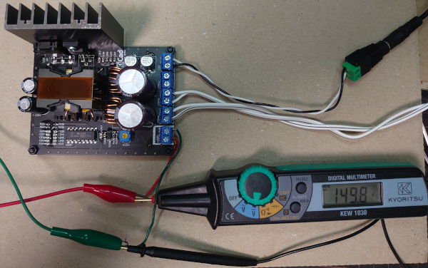
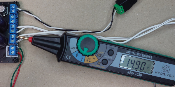
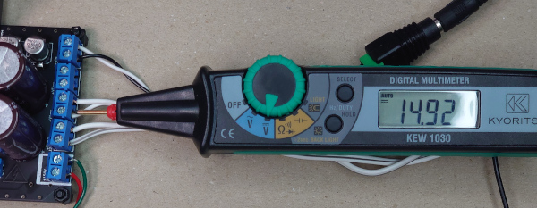
まあ設計通りの性能がでているんじゃないかな。。。
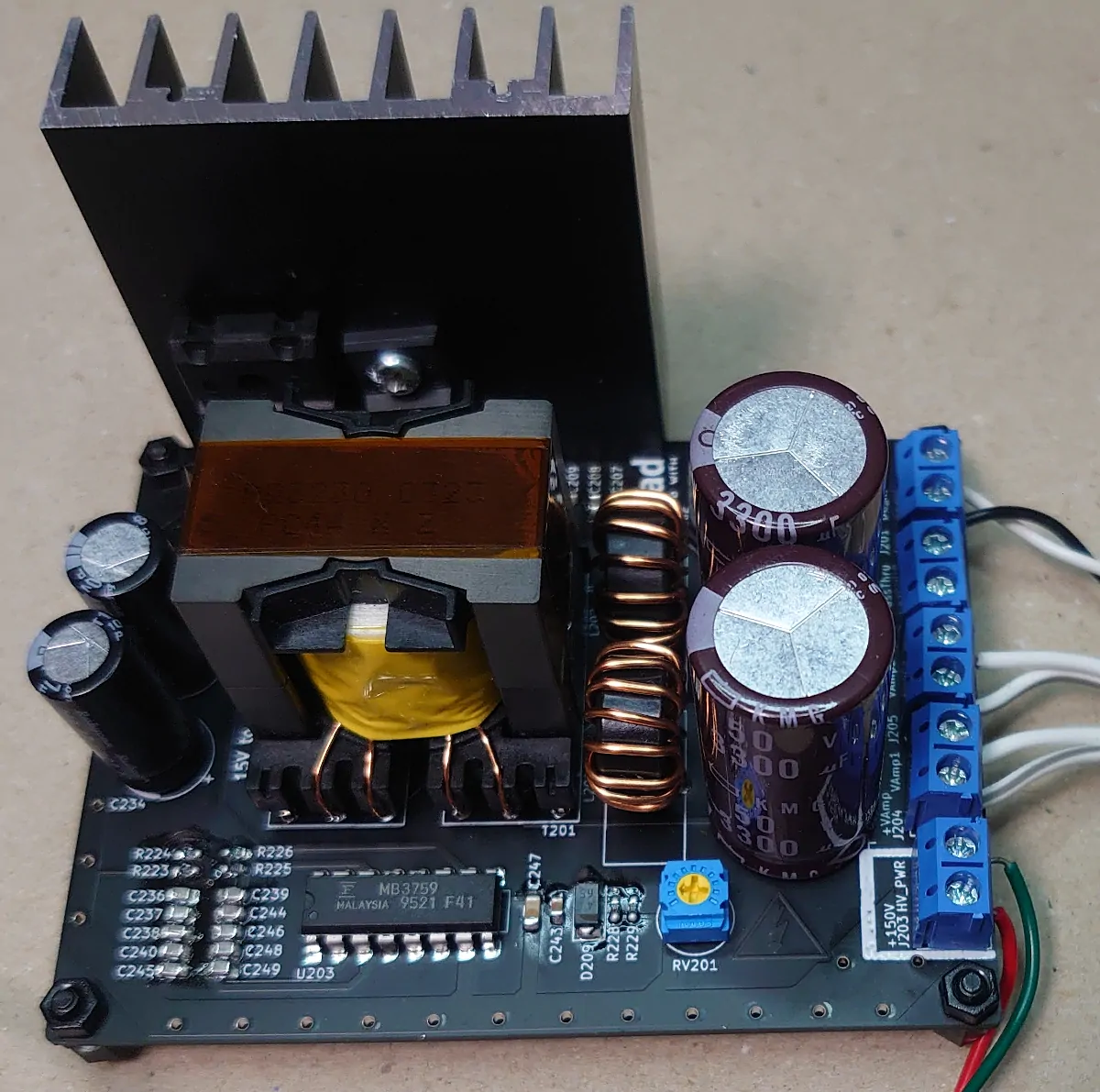
ということで前に作った巨人版ヘッドホンアンプにこの+-15V電源をつないで音を出そう。
入力はACアダプタによる 15V
まあ設計通りの性能がでているんじゃないかな。。。
ということで前に作った巨人版ヘッドホンアンプにこの+-15V電源をつないで音を出そう。
著者: Akihiro Yamamoto
リンク: https://ak1211.com/posts/7610/
ライセンス: CC BY-NC-SA 4.0
This work is licensed under a Creative Commons Attribution-NonCommercial-ShareAlike 4.0 International License. Please attribute the source, use non-commercially, and maintain the same license.
キーワードを入力して記事を検索
コメント